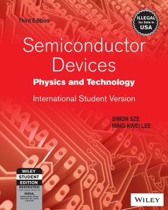
Semiconductor Devices, Physics and Technology, 3ed, ISV
ISBN: 9788126556755
592 pages
Publication Year: 2015
eBook also available for institutional users
For more information write to us at: acadmktg@wiley.com

Description
This book is an introduction to the physical principles of modern semiconductor devices and their advanced fabrication technology. It begins with a brief historical review of major devices and key technologies and is then divided into three sections: semiconductor material properties, physics of semiconductor devices and processing technology to fabricate these semiconductor devices.
Preface
Acknowledgments
Chapter 0 1 Introduction
0.1 Semiconductor Devices
0.2 Semiconductor Technology
Part I Semiconductor Physics
Chapter 1 Energy Bands and Carrier Concentration in Thermal Equilibrium
1.1 Semiconductor Materials
1.2 Basic Crystal Structures
1.3 Valence Bonds
1.4 Energy Bands
1.5 Intrinsic Carrier Concentration
1.6 Donors and Acceptors
Chapter 2 Carrier Transport Phenomena
2.1 Carrier Drift
2.2 Carrier Diffusion
2.3 Generation and Recombination Processes
2.4 Continuity Equation
2.5 Thermionic Emission Process
2.6 Tunneling Process
2.7 Space-Charge Effect
2.8 High-Field Effects
Part II Semiconductor Devices
Chapter 3 p-n Junction
3.1 Thermal Equilibrium Condition
3.2 Depletion Region
3.3 Depletion Capacitance
3.4 Current-Voltage Characteristics
3.5 Charge Storage and Transient Behavior
3.6 Junction Breakdown
3.7 Heterojunction
Chapter 4 Bipolar Transistors and Related Devices
4.1 Transistor Action
4.2 Static Characteristics of Bipolar Transistors
4.3 Frequency Response and Switching of Bipolar Transistors
4.4 Nonideal Effects
4.5 Heterojunction Bipolar Transistors
4.6 Thyristors and Related Power Devices
Chapter 5 MOS Capacitor and MOSFET
5.1 Ideal MOS Capacitor
5.2 SiO2-Si MOS Capacitor
5.3 Carrier Transport in MOS Capacitors
5.4 Charge-Coupled Devices (CCD)
5.5 MOSFET Fundamentals
Chapter 6 Advanced MOSFET and Related Devices
6.1 MOSFET Scaling
6.2 CMOS and BiCMOS
6.3 MOSFET on Insulator
6.4 MOS Memory Structures
6.5 Power MOSFET
Chapter 7 MESFET and Related Devices
7.1 Metal-Semiconductor Contacts
7.2 MESFET
7.3 MODFET
Chapter 8 Microwave Diodes; Quantum-Effect and Hot-Electron Devices
8.1 Microwave Frequency Bands
8.2 Tunnel Diode
8.3 IMPATT Diode
8.4 Transferred-Electron Devices
8.5 Quantum-Effect Devices
8.6 Hot-Electron Devices
Chapter 9 Light Emitting Diodes and Lasers
9.1 Radiative Transitions and Optical Absorption
9.2 Light-Emitting Diodes
9.3 Various Light-Emitting Diodes
9.4 Semiconductor Lasers
Chapter 10 Photodetectors and Solar Cells
10.1 Photodetectors
10.2 Solar Cells
10.3 Silicon and Compound-Semiconductor Solar Cells
10.4 Third-Generation Solar Cells
10.5 Optical Concentration
Part III Semiconductor Technology
Chapter 11 Crystal Growth and Epitaxy
11.1 Silicon Crystal Growth from the Melt
11.2 Silicon Float-Zone Process
11.3 GaAs Crystal-Growth Techniques
11.4 Material Characterization
11.5 Epitaxial-Growth Techniques
11.6 Structures and Defects in Epitaxial Layers
Chapter 12 Film Formation
12.1 Thermal Oxidation
12.2 Chemical Vapor Deposition of Dielectrics
12.3 Chemical Vapor Deposition of Polysilicon
12.4 Atom Layer Deposition
12.5 Metallization
Chapter 13 Lithography and Etching
13.1 Optical Lithography
13.2 Next-Generation Lithographic Methods
13.3 Wet Chemical Etching
13.4 Dry Etching
Chapter 14 Impurity Doping
14.1 Basic Diffusion Process
14.2 Extrinsic Diffusion
14.3 Diffusion-Related Processes
14.4 Range of Implanted Ions
14.5 Implant Damage and Annealing
14.6 Implantation-Related Processes
Chapter 15 Integrated Devices
15.1 Passive Components
15.2 Bipolar Technology
15.3 MOSFET Technology
15.4 MESFET Technology
15.5 Challenges for Nanoelectronics
Appendix A List of Symbols
Appendix B International Systems of Units (SI Units)
Appendix C Unit Prefixes
Appendix D Greek Alphabet
Appendix E Physical Constants
Appendix F Properties of Important Element and Binary Compound Semiconductors at 300 K
Appendix G Properties of Si and GaAs at 300 K
Appendix H Derivation of the Density of States in a Semiconductor
Appendix I Derivation of Recombination Rate for Indirect Recombination
Appendix J Calculation of the Transmission Coefficient for a Symmetric Resonant-Tunneling Diode
Appendix K Basic Kinetic Theory of Gases
Appendix L Answers to Selected Problems
Photo credits
Index

